


Date
29 Sep 2018
Workshop on VLSI Design
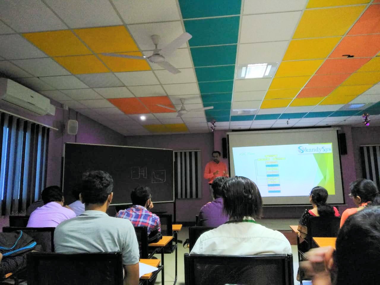
Resource Person : Mr. Vaibhav Raj Purohit, Team Leader, Skandysys Technologies,Bangalore
Date : 29th September 2018
Time : 09:30 AM to 4:00 PM
Venue : Seminar Hall-1
No. of Participants : ECE students (31) + Staff (08)
Outcome of the Program :The Technical Talk started with welcoming of Mr. Vaibhav Raj purohit, Team Leader, Skandysys Technologies by Dr.M. Mathivanan by presenting a bouquet. The Speaker himself introduced about his Qualification, Current working area and about his company. He also explained about the present scenario in industries and their expectations etc. Next, he started with the design of process of a producing a packed VLSI chip physically and various steps which is popularity known as VLSI design cycle. This design cycle is normally represented as a step as shown in below
- System specification
- Functional design
- Logic design
- Circuit design
- Physical design
- Fabrication
- Packaging
System specification: The specification of the system to be designed exactly specified in this step. It considers performance, functionality and the physical dimensions of the design
Functional design: In this step, behavioural aspects of the system and considered. The outcome is usually a timing diagram or other relationship
Logic design: In this step, the functional design is converted into a logic design, using the Boolean. These expressions are minimizing to achieve the smallest logic design
Circuit design: The step involves conversion of boolean expression into a circuit representation by taking into consideration of speed and power
Physical design: In this step, the circuit representation of each component is converted a geometric representation
Design verification: In this step, the layout is verified to ensure the layout meets the system specification and fabrication requirements
Fabrication: This step is followed design verification the fabrication power consists of several steps like preparation of wafer, deposition.
The theory part was done in Morning Session, and afternoon hands on experience in the VLSI Lab was conducted for the students explaining in details the steps involved in VLSI design. The students are very much benefitted from the workshop.


Events List
- Career Guidance Session on “Exploring Opportunities Abroad”
- CSE 3rd Semester VTU Examination Result (December 2024)
- Industrial Visit to Bangalore Aircraft Industries Pvt. Ltd., Bengaluru
- 4-Day Student Development Program on “Generative AI in Healthcare Applications”
- International Women’s Day Celebration
- Expert Talk on Soft Skills & Interview Skills Development.
- Seminar on “Embedded Systems and Automotive Software (AI & Gen AI)”
- Seminar on “AICTE Funding Opportunities and the Need for Incubation Cells at HEIs”
- Guest lecture on Advancements in Space Propulsion
- Seminar on Composite Materials for Aircraft Structures